 English
 日本語
日本語 русский
 Español
 Deutsch
 中文简体
中文简体Content
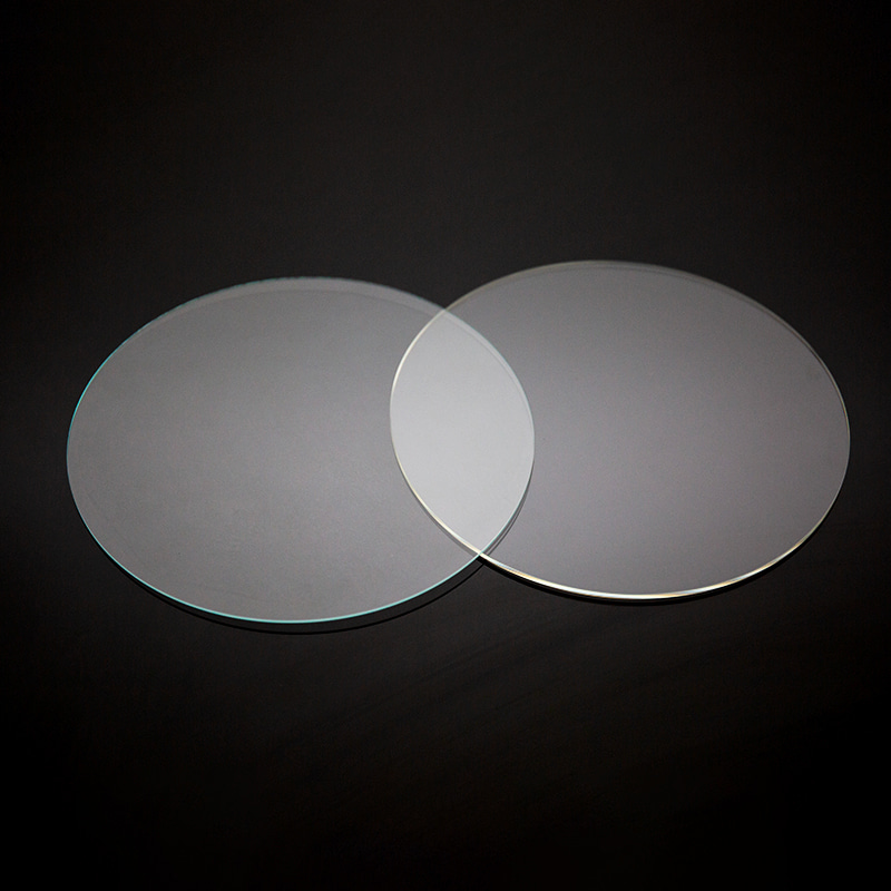
Flatness is a critical parameter in the fabrication of optical wafers. Optical wafers serve as fundamental components in a wide array of applications, including photonics, lasers, optical sensors, and high-precision lens systems. Any deviation from flatness can compromise the performance of the device, introduce optical aberrations, and reduce manufacturing yield. Ensuring wafer flatness is therefore essential to maintain both quality and functionality.
Understanding Optical Wafer Flatness
Optical wafer flatness refers to the uniformity of the wafer surface along its plane. Deviations from an ideal flat plane can occur as bowing, warping, or surface undulations. These variations can be measured using several parameters, including total thickness variation, surface profile, and global flatness metrics. Typically, flatness is expressed in micrometers, with tighter tolerances required for high-precision optical applications.
The importance of flatness arises from the need for predictable light propagation through the wafer. Even minor surface deviations can distort light beams, reduce laser efficiency, or impair optical coatings. Therefore, flatness is not only a quality metric but also a functional requirement.
Factors Affecting Optical Wafer Flatness
Several factors influence wafer flatness during fabrication. These factors can be broadly categorized into material properties, mechanical processing, and environmental conditions.
Material Properties
The choice of material plays a significant role in wafer flatness. Optical wafers are typically made from crystalline materials such as silicon, gallium arsenide, or sapphire, each of which has unique thermal and mechanical characteristics. Differences in thermal expansion coefficients, internal stresses, and crystal defects can induce warping. For example, anisotropic expansion in crystalline wafers can cause bowing if the wafer is not properly oriented along the crystal axes.
Mechanical Processing
Mechanical processing steps, including slicing, grinding, and polishing, directly influence wafer flatness. Slicing a crystal from a boule introduces mechanical stresses that can warp the wafer. Similarly, grinding operations remove material to achieve the desired thickness but can introduce uneven stress distribution. Polishing, which is essential for optical surface quality, can correct some of these deviations if performed carefully but can also introduce micro-bending if not controlled properly.
Environmental Conditions
Environmental factors, such as temperature, humidity, and vibrations, affect wafer flatness. During fabrication, wafers can absorb moisture or experience thermal gradients, causing temporary or permanent deformation. Maintaining a controlled cleanroom environment is essential to mitigate these effects and preserve flatness.
Techniques to Ensure Flatness
Ensuring flatness in optical wafer fabrication involves a combination of material selection, precision processing, and metrology. Several techniques are commonly employed to achieve and verify flatness.
1. Careful Material Selection
The first step in ensuring wafer flatness is selecting high-quality raw materials. Boules should be free from internal defects and carefully oriented to minimize anisotropic effects. Using low-stress crystals reduces the likelihood of warping during slicing and subsequent processing.
2. Precision Slicing
Wafer slicing involves cutting thin wafers from the bulk crystal using wire saws or diamond-coated blades. Precision slicing reduces mechanical stress by maintaining uniform contact and avoiding thermal shock. Advanced slicing methods, such as diamond wire saws with optimized feed rates, minimize micro-cracks and edge damage that could lead to uneven surfaces.
3. Controlled Grinding
Grinding is performed to achieve the target thickness and improve surface flatness. Double-side grinding, in which both sides of the wafer are processed simultaneously, ensures that material removal is uniform. This technique minimizes bowing and reduces residual stress. Modern grinding machines use computer-controlled pressure and speed settings to achieve consistent results across multiple wafers.
4. Polishing Techniques
Polishing is a critical step in achieving optical flatness. Chemical-mechanical polishing combines mechanical abrasion with chemical reactions to produce ultra-flat surfaces. The polishing process must be carefully monitored to avoid introducing new stresses. Polishing pads and slurry compositions are optimized for uniform material removal, ensuring that the wafer surface remains within the specified flatness tolerance.
5. Stress Relief and Annealing
Thermal treatments can relieve internal stresses in optical wafers. Annealing involves heating the wafer to a specific temperature and then cooling it slowly. This process allows the crystal lattice to relax, reducing bowing and warping. Proper annealing schedules are crucial, as excessive or uneven heating can exacerbate flatness issues.
6. Metrology and Inspection
Accurate measurement of wafer flatness is essential to monitor fabrication quality. Interferometry, profilometry, and laser scanning are commonly used techniques to detect deviations at the micrometer or sub-micrometer level. Early detection of flatness issues allows for corrective actions, such as additional polishing or selective material removal, before wafers progress to further stages of fabrication.
7. Environmental Control
Maintaining a stable fabrication environment is crucial for preserving wafer flatness. Cleanrooms with controlled temperature and humidity reduce the risk of thermal expansion and moisture-induced warping. Anti-vibration platforms and carefully designed storage systems prevent mechanical deformation during handling and transport.
Challenges in Maintaining Flatness
Despite advanced techniques, several challenges persist in ensuring optical wafer flatness. High wafer diameters increase susceptibility to bowing, as larger wafers experience greater stress gradients. Thin wafers are more prone to bending under their own weight or during handling. Furthermore, complex wafer geometries, such as patterned or coated wafers, may introduce localized stress points that compromise flatness.
Another challenge is the trade-off between surface flatness and material removal rate. Aggressive grinding and polishing can increase throughput but may introduce micro-stresses. Balancing productivity with high-precision requirements remains a critical consideration for manufacturers.
Advances in Flatness Control
Recent technological advances have improved the ability to achieve ultra-flat optical wafers. Real-time monitoring systems track material removal during grinding and polishing, allowing automatic adjustments to maintain flatness. Adaptive polishing techniques, which vary pressure and slurry flow dynamically, compensate for local thickness variations. Additionally, advances in wafer bonding and substrate engineering reduce stress-induced deformation in composite optical wafers.
Practical Considerations for Manufacturers
For manufacturers, ensuring wafer flatness is a multi-step process that requires integration across all fabrication stages. From selecting high-quality crystal boules to employing precision slicing, grinding, polishing, and stress relief, every step contributes to the final flatness. Continuous inspection and environmental control are also essential to maintain consistency across production batches.
Investing in high-precision equipment and trained personnel is essential for achieving the desired flatness. Standardized protocols and adherence to flatness specifications ensure that wafers meet the performance requirements for high-end optical applications.
Conclusion
Flatness in optical wafer fabrication is a fundamental quality parameter that affects the performance of optical devices and systems. Achieving and maintaining flatness requires careful attention to material selection, mechanical processing, thermal treatments, and environmental control. Advanced metrology and adaptive processing techniques further enhance the ability to produce wafers that meet stringent flatness requirements.
Understanding the factors that influence flatness and implementing robust fabrication and inspection processes are essential for manufacturers and researchers working with optical wafers. By prioritizing flatness, optical wafers can reliably meet the high-precision demands of modern photonics, laser systems, and optical sensing applications.


 苏公网安备32041102000130号