 English
 日本語
日本語 русский
 Español
 Deutsch
 中文简体
中文简体


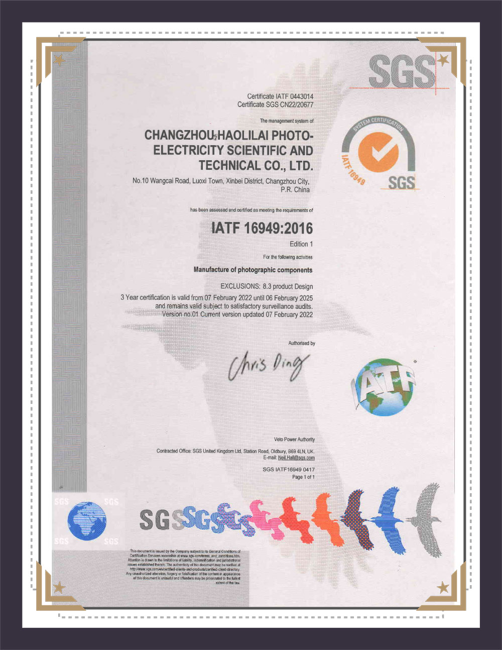
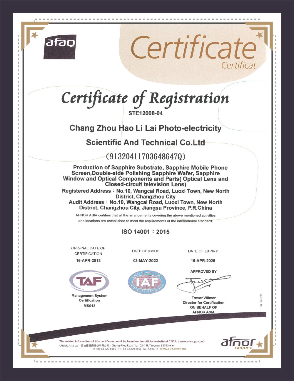
Founded in 1998, HLL is China Optical Wafers Manufacturers and Optical Wafers suppliers, located in the national-level High-tech Development District, Changzhou, Jiangsu, China. It’s neighboring Shanghai-Nanjing Expressway on the north, Changzhou high-speed railway station on the east, Changzhou Airport on the west. HLL covers an area of 35,000m² and has passed the system certification such as ISO9001:2015, ISO14001:2015, and IATF16949.
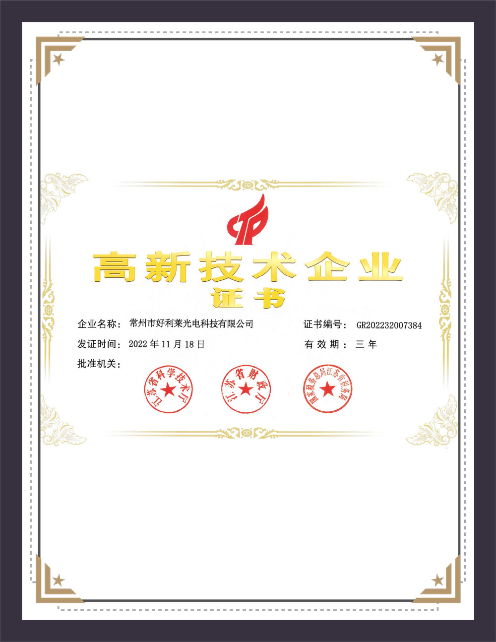
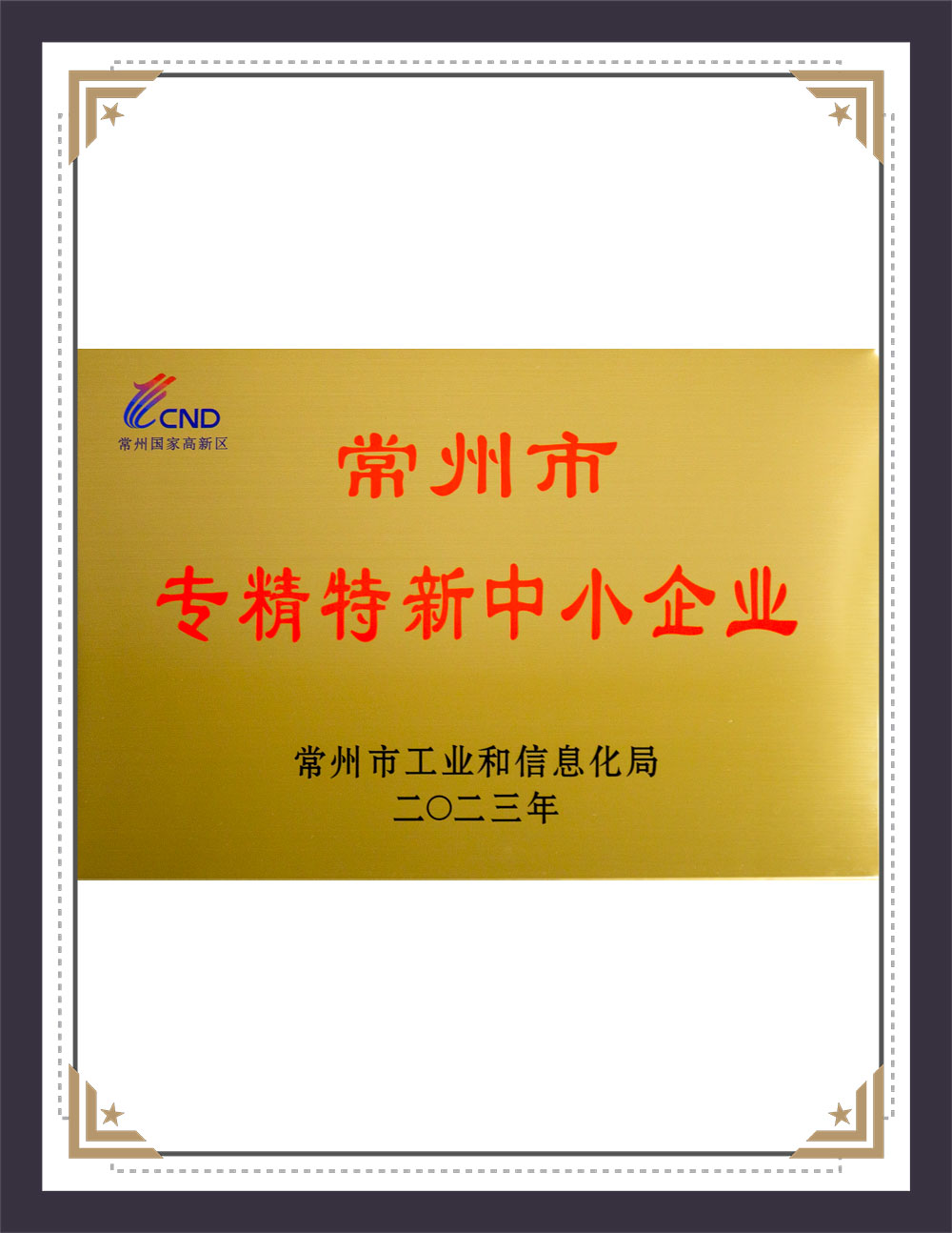
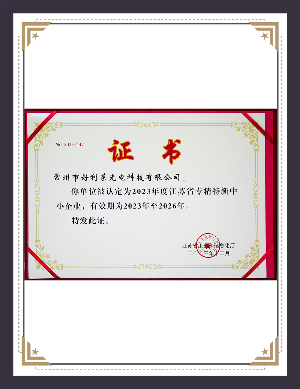
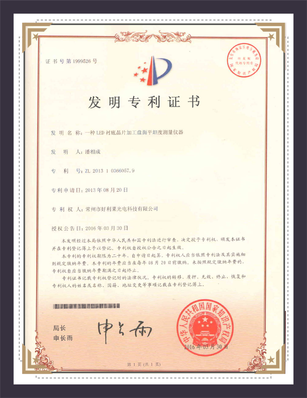
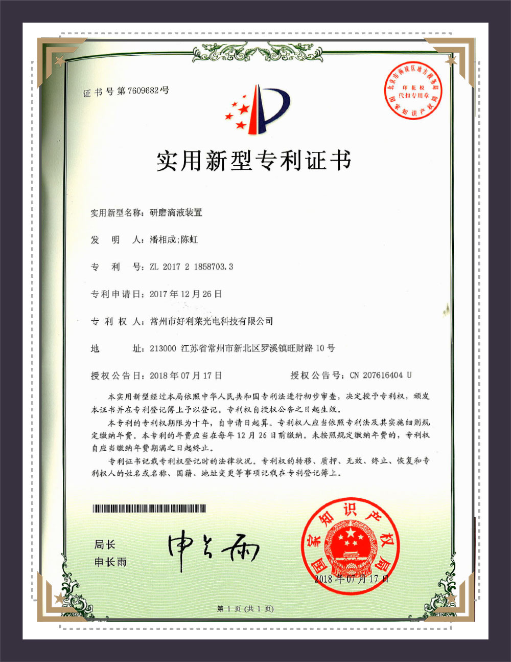
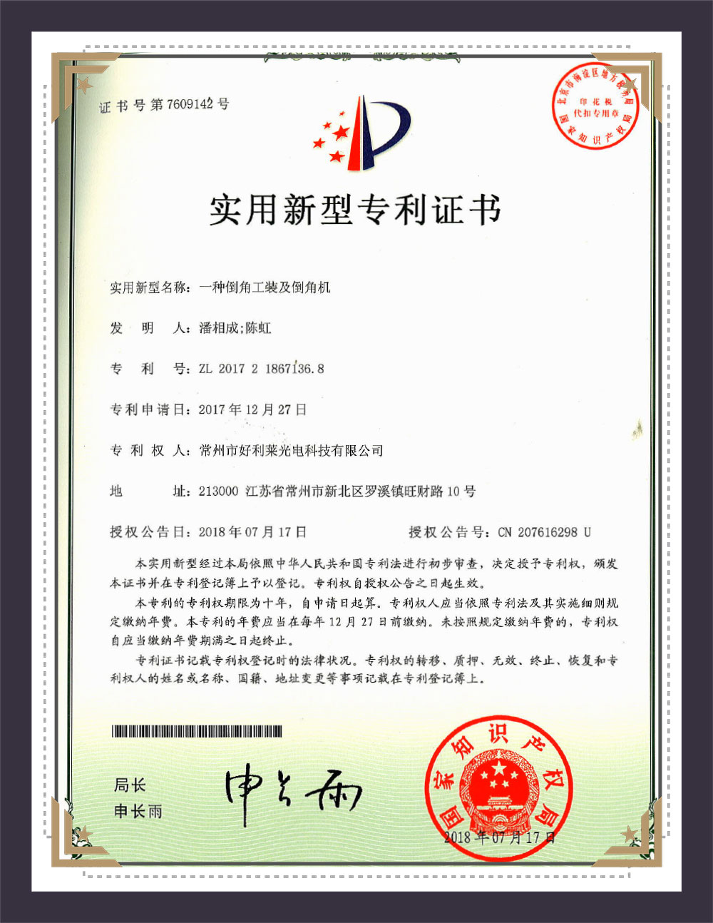
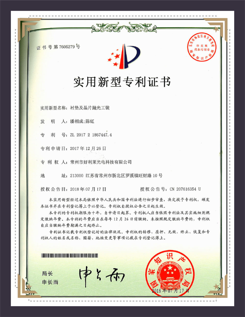
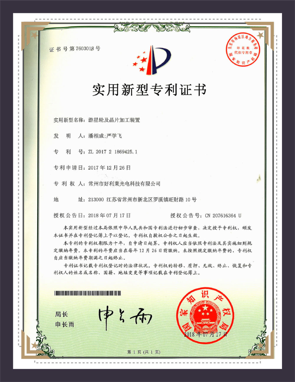
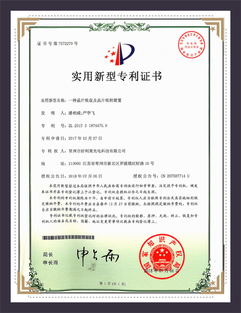
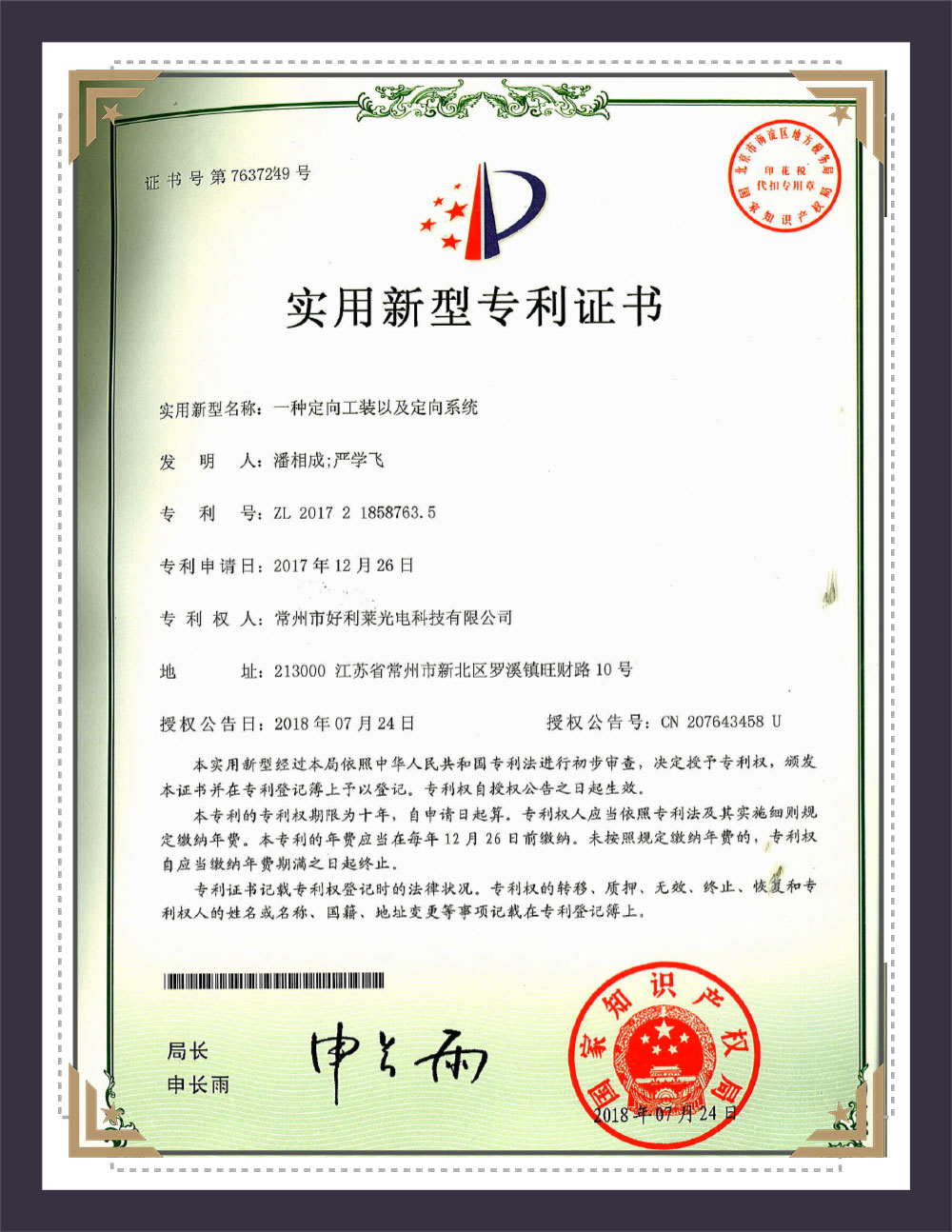
As a High-Tech enterprise in Jiangsu province, HLL boasts a talented team with intensive experience and professional technology. HLL has established Jiangsu Precision Optical Lens Engineering Technology Center and Jiangsu Enterprise Technology Research Center and obtained multiple patents for inventions, multiple utility model patents and multiple Jiangsu High New Tech Products.
HLL mainly develops and produces various precision optical components. Focus on laser optics, auto optics, the semiconductor industry and consumer optics. HLL will strive to become a benchmark in China's optical industry.
Optical Wafers Manufacturers
HLL manufactures wafers processed from sapphire, glass, and quartz, with dimensions mainly available in 4 inches, 6 inches, 8 inches, and 12 inches. They are widely used in the semiconductor and consumer electronics industries.
About Us
Changzhou Haolilai Photo-Electricity Scientific and Technical Co., Ltd.
Certificate & Honor
News
-
Direct Answer to Your Quartz Wafer Needs A quartz wafer is a thin, precisely cut slice of single-crystal quartz that forms the backbone of countless ...
READ MORE -
Key Differentiators in Optical Lens Engineering The fundamental distinction between an optical automotive lens and an optical laser lens lies in thei...
READ MORE -
Matching the Filter to the Measurement Goal Achieving reliable contrast and spectral purity in any optical setup depends on one component: the optica...
READ MORE -
An optical prism transforms a light beam’s direction and spectral composition through controlled refraction and reflection. The most familiar result i...
READ MORE
Message Feedback
Wafer Industry knowledge
How do optical wafers power everyday devices?
In the fast-paced world of technology, optical wafers play a crucial role in powering the devices we use every day. From smartphones to smartwatches, these tiny but mighty components are the unsung heroes behind the scenes.
Optical wafers, also known as silicon wafers, are thin, circular discs made from purified silicon crystals. These wafers are the building blocks of integrated circuits, which are essential components in electronic devices. The process of manufacturing optical wafers involves several intricate steps, including crystal growth, wafer slicing, polishing, and doping. Each wafer can contain hundreds of individual chips, each with its own unique function.
One of the key reasons optical wafers are widely used in electronics is their ability to handle high temperatures and provide excellent electrical conductivity. This makes them ideal for applications where reliability and performance are paramount, such as in aerospace, medical devices, and telecommunications equipment. Optical wafers are also incredibly versatile, with manufacturers constantly pushing the boundaries of what is possible with new innovations and designs.
As technology continues to advance, the demand for smaller, faster, and more powerful devices is on the rise. This has led to a growing need for optical wafers that can support increasingly complex integrated circuits. Engineers and researchers are constantly exploring new materials and manufacturing techniques to keep up with these demands. The future of optical wafers holds exciting possibilities, from flexible electronics to quantum computing.
Optical wafers may be small in size, but their impact on the world of technology is immense. As we rely more and more on electronic devices in our daily lives, the importance of these tiny silicon discs cannot be overstated. The next time you pick up your smartphone or use a smart home device, take a moment to appreciate the incredible technology packed into these compact packages. Optical wafers truly are the unsung heroes that keep our world connected and running smoothly.
- Address: No.10 wangcai road, Luoxi town,Xinbei district, Changzhou,Jiangsu, China.
- Phone: +86-519-83200018
- E-mail: [email protected]
COPYRIGHT 2024 Changzhou Haolilai Photo-Electricity Scientific and Technical Co., Ltd. ALL RIGHTS RESERVED.
 Wholesale Optical Wafers Factory Privacy
 苏公网安备32041102000130号