 English
 日本語
日本語 русский
 Español
 Deutsch
 中文简体
中文简体Content
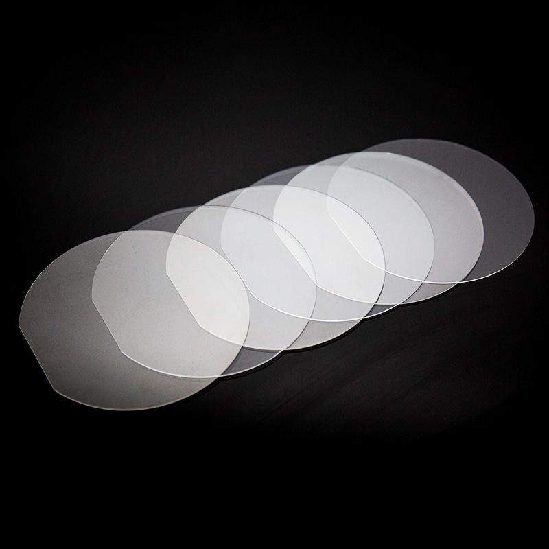
Optical wafers are essential components in various high-tech industries, including telecommunications, semiconductor manufacturing, and photonics. These thin, disc-shaped substrates are used to create optical devices such as lenses, filters, and sensors. Understanding their properties, applications, and manufacturing processes can help engineers and researchers optimize their use in advanced technologies.
What Are Optical Wafers?
Optical wafers are ultra-thin, flat substrates typically made from materials like silicon, glass, or specialized optical crystals. They serve as the foundation for fabricating micro-optical elements, including:
- Diffractive optical elements (DOEs)
- Waveguides
- Optical filters
- Photonic integrated circuits (PICs)
Their precision and material properties determine their performance in applications such as laser systems, imaging devices, and fiber optics.
Key Materials for Optical Wafers
The choice of material depends on the intended application, wavelength range, and environmental conditions. Below is a comparison of common optical wafer materials:
| Material | Key Properties | Common Applications |
| Silicon (Si) | High refractive index, IR-transparent | Infrared optics, photodetectors |
| Fused Silica | Low thermal expansion, UV-transparent | Laser optics, lithography |
| Sapphire (Al₂O₃) | Extreme hardness, scratch-resistant | LED substrates, harsh environments |
| Gallium Arsenide (GaAs) | High electron mobility | High-frequency photonics, lasers |
Each material offers unique advantages, making it crucial to select the right one based on optical and mechanical requirements.
Manufacturing Process of Optical Wafers
Producing high-quality optical wafers involves several precision steps:
- Material Selection – Choosing the right substrate based on optical and thermal properties.
- Wafer Slicing – Cutting ingots into thin wafers using diamond saws or laser cutting.
- Polishing – Achieving nanometer-level surface smoothness to minimize light scattering.
- Coating (Optional) – Applying anti-reflective or dielectric coatings for enhanced performance.
- Dicing & Etching – Shaping the wafer into smaller components for integration into devices.
Precision is critical at every stage, as defects can degrade optical performance.
Applications of Optical Wafers
Optical wafers are used in a wide range of industries:
1. Telecommunications
- Fiber optic networks rely on optical wafers for signal routing and amplification.
- Wavelength division multiplexing (WDM) systems use wafer-based filters to separate light channels.
2. Semiconductor Industry
- Photolithography uses fused silica wafers to pattern microchips with extreme precision.
- Silicon wafers are essential for photonic integrated circuits (PICs).
3. Medical & Biotech
- Optical biosensors detect molecular interactions in lab-on-a-chip devices.
- Endoscopic imaging systems incorporate micro-optical elements for high-resolution diagnostics.
4. Defense & Aerospace
- Infrared optical wafers enable thermal imaging and laser targeting systems.
- Sapphire wafers are used in ruggedized sensors for harsh environments.
Key Considerations When Choosing Optical Wafers
Selecting the right optical wafer involves evaluating several factors:
- Wavelength Range – Ensure the material transmits light at the desired wavelengths.
- Thermal Stability – Some applications require resistance to high temperatures.
- Surface Quality – Scratches or impurities can cause light scattering.
- Cost vs. Performance – High-performance materials may be expensive but necessary for critical applications.
Future Trends in Optical Wafer Technology
Advancements in optical wafer technology are driving innovation in multiple fields:
- Miniaturization – Thinner wafers enable compact photonic devices.
- New Materials – Emerging compounds like silicon nitride (Si₃N₄) improve performance in photonics.
- Hybrid Integration – Combining different materials (e.g., silicon and lithium niobate) enhances functionality.
Conclusion
Optical wafers play a pivotal role in modern optoelectronics, photonics, and telecommunications. Their material properties, manufacturing precision, and application versatility make them indispensable in cutting-edge technologies. By understanding their characteristics and selection criteria, engineers and researchers can optimize their use in next-generation optical systems.


 苏公网安备32041102000130号