
 Search
 en
en English
 日本語
日本語 русский
 Español
 Deutsch
 中文简体
中文简体Content
Direct Answer to Your Quartz Wafer Needs
A quartz wafer is a thin, precisely cut slice of single-crystal quartz that forms the backbone of countless precision electronic and optical devices. Its unmatched combination of the piezoelectric effect, a quality factor routinely exceeding 1 million, and broad optical transparency makes it the default substrate for frequency control, sensing, and high-stability timing circuits. Simply put, if an application demands a stable mechanical resonance with minimal energy loss or a durable, low-fluorescence window for ultraviolet light, a properly specified quartz wafer is almost always the right starting point.
What Exactly Is a Quartz Wafer
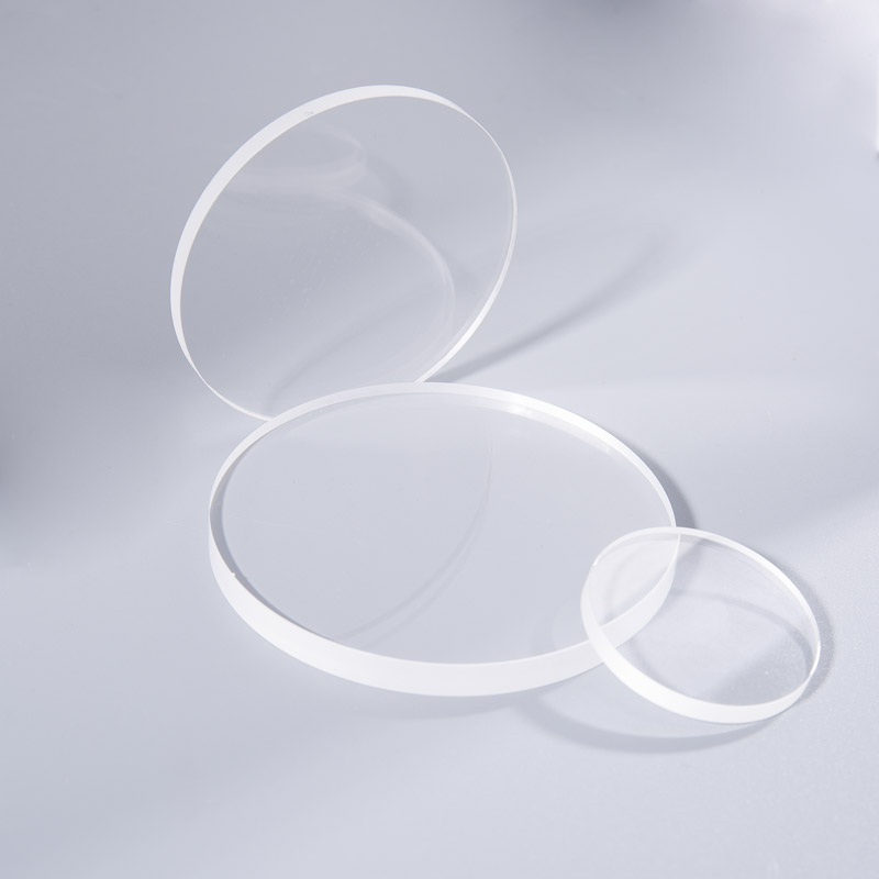
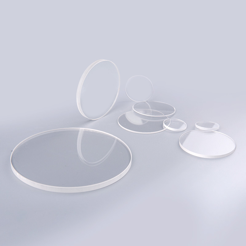
A quartz wafer is a flat, parallel-faced plate cut from a synthetically grown quartz crystal bar. The material is silicon dioxide in its alpha-quartz phase, which remains stable up to 573 degrees Celsius. The crystal orientation of the cut determines how the wafer vibrates under an electric field. Typical wafer diameters range from 2 inches to 6 inches in production, with thicknesses spanning from a few tens of microns for high-frequency resonators to several millimeters for optical delay plates.
Unlike polycrystalline ceramics or amorphous glass, a single-crystal quartz wafer delivers an extrinsic Q factor of over 10^6 in vacuum, which directly translates to oscillator phase noise below -160 dBc/Hz at 10 kHz offset. That performance is why quartz-based oscillators still dominate 5G base stations, satellite communications, and precision instrumentation despite the emergence of silicon MEMS alternatives.
Critical Properties That Define Performance
Every design decision around a quartz wafer starts with its anisotropic nature. The piezoelectric, elastic, and thermal expansion coefficients change dramatically with the angle of the cut. The table below summarizes the most widely used crystal cuts and the typical stability they offer.
| Crystal Cut | Primary Vibration Mode | Temperature Stability | Key Application |
|---|---|---|---|
| AT-cut | Thickness shear | ±5 ppm over 0–50 °C | Oscillators, filters, sensors |
| SC-cut | Thickness shear | ±10 ppm over -40–90 °C | OCXOs, high-stress environments |
| BT-cut | Thickness shear | Higher frequency constant | High-frequency fundamental-mode resonators |
| ST-cut | Surface acoustic wave | Zero first-order temperature coefficient at 25 °C | SAW filters, delay lines |
Beyond the cut, surface quality and geometric tolerances define the wafer's insertion loss and spurious mode suppression. A double-side polished AT-cut wafer with a surface roughness below 0.5 nm Ra and a total thickness variation under 2 µm will reliably excite the intended overtone without scattering acoustic energy into unwanted modes.
Where Quartz Wafers Make the Difference
Frequency Control and Timing
More than 90 percent of all electronic clocks and microcontrollers rely on a quartz wafer resonator. The wafer is metalized with electrodes, packaged, and driven into resonance. An AT-cut wafer 100 µm thick oscillates at a fundamental frequency of approximately 16.7 MHz, and overtone polishing allows stable operation at the 3rd or 5th overtone well into the VHF range. This scalability is why a single quartz wafer can serve both a 32.768 kHz tuning fork watch crystal and a 100 MHz oven-controlled crystal oscillator.
Sensing and Microbalances
A quartz crystal microbalance using an AT-cut wafer can detect mass changes as small as 0.1 ng/cm². The wafer serves as the acoustic resonator, and any mass added to its surface proportionally shifts the resonant frequency. This principle is exploited in thin-film deposition monitors, gas sensors, and biomedical assays where label-free detection is critical.
Optical and High-Energy Applications
Quartz wafers transmit from the deep ultraviolet to the near infrared, typically from 160 nm to 3 µm. Their low auto-fluorescence and high laser damage threshold make them standard windows in excimer laser systems and UV spectroscopy. A laser-grade polished surface with a scratch-dig specification of 10-5 and a flatness of lambda/10 at 633 nm is commonly requested for these optical duties.
How a High-Purity Quartz Wafer Is Made
The process begins with hydrothermal growth in an autoclave. Nutrient quartz dissolves in an alkaline solution at around 350 degrees Celsius and 1,500 bar, then recrystallizes onto oriented seed plates over several months. The resulting synthetic crystal bars have an aluminum impurity level below 10 ppm, a critical parameter since aluminum-hole centers cause radiation-induced frequency shifts.
Wafering follows a strict sequence:
- X-ray orientation and dicing to within 0.1 degree of the specified cut angle
- Lapping with progressively finer alumina slurries to remove sub-surface damage
- Edge rounding to prevent chipping during handling and electrode deposition
- Chemical-mechanical polishing to achieve the required mirror finish
- Final cleaning and inspection under diffuse laser light to flag any scratches or pits larger than 1 µm
Quality Grades and Inspection Standards
Not every application demands the same wafer grade. The following categories help align cost with performance:
- Electronic grade: Double-side polished, TTV below 2 µm, orientation accuracy better than 0.5 degree. Designed for high-Q resonators and filters.
- Optical grade: Laser-grade polish on one or both faces, 10-5 scratch-dig, lambda/10 flatness. Used for UV windows and waveplates.
- Research grade: As-cut or single-side polished wafers with looser thickness tolerances, suitable for prototyping and thin-film depositions where a reference surface is enough.
Incoming quality control typically includes a white light interferometer scan for surface roughness, a stylus profiler for TTV, and an X-ray rocking curve measurement to confirm the crystallographic orientation within the specified tolerance.
How to Select the Right Quartz Wafer
The decision tree is straightforward once the application is clear. Follow these steps to avoid costly mismatches:
- Define the cut first. For room-temperature frequency control with minimal complexity, AT-cut is the default. If the oscillator will sit in an OCXO with a fast warm-up requirement, the SC-cut's immunity to thermal transient effects justifies the higher cost.
- Lock in the frequency or thickness. The equation f = 1.66 mm·MHz / thickness guides AT-cut design. A 0.33 mm thick wafer gives a 5 MHz fundamental, while a 0.083 mm wafer reaches 20 MHz.
- Specify surface finish. For resonator electrodes, a double-side polished wafer with Ra below 0.5 nm is essential. For optical transmission, add the scratch-dig and flatness requirements as per the laser wavelength.
- Check the diameter and flat alignment. Many automated assembly lines require a primary flat of a specific length and crystallographic orientation to guarantee repeatable electrode alignment.
With these parameters defined, a procurement specification for a typical AT-cut oscillator wafer might read: AT-cut, 13.5 mm diameter, 0.137 mm thick, double-side polished, Ra under 0.4 nm, orientation accuracy within 0.25 degree, and no scratches visible at 50x magnification. That level of detail ensures the wafer will perform as expected from the first prototype to mass production.

 苏公网安备32041102000130号