
 Search
 en
 English
 日本語
 русский
 Español
 Deutsch
 中文简体
Content
What a Sapphire Wafer Actually Is
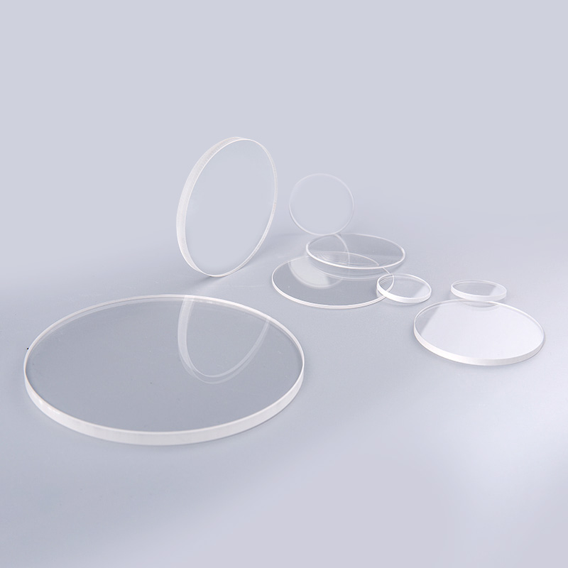
A sapphire wafer is a thin disc of single-crystal aluminum oxide that has been oriented to a crystallographic plane, cored from a grown boule, sliced, lapped, and polished to a controlled thickness, flatness, and surface finish.
Sapphire is neither glass nor a coating. It is crystalline Al2O3, the material of corundum, which is why a finished wafer combines Mohs 9 hardness with a band gap near 8.6 eV and useful transmission from roughly 0.19 to 5.5 micrometers.
Orientation is the first decision on any drawing, because it fixes what can be grown on the surface and how the wafer behaves under thermal load.
- c-plane (0001): the default for GaN LED and microLED epitaxy, where the hexagonal surface matches the epilayer.
- r-plane: used for silicon-on-sapphire, where a thin silicon film is deposited heteroepitaxially.
- a-plane and m-plane: non-polar research orientations, available but harder to polish to the same roughness.
- Offcut: 0.2 degrees toward the a-axis is a common MOCVD request, while 4 degrees appears in specific device work. Hold the tolerance tightly, because offcut drift changes step structure during growth.
Diameter and thickness travel together. Common sizes are 50.8 mm, 100 mm, 150 mm, and 200 mm, with thickness rising from about 430 micrometers at 2 inch to 650 at 4 inch and above 1 mm at 6 inch, simply because a thin disc of a brittle crystal will not survive routine handling.
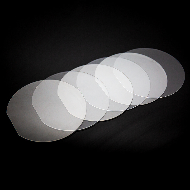 Sapphire Wafers in Common Diameters and ThicknessesReview single-crystal sapphire wafer options from 2 to 8 inches, with thickness, surface, and flatness specifications for optoelectronic and LED substrates.View Product →
From Boule to Epi-Ready Wafer
Sapphire wafers are produced in six stages, and each stage leaves a fingerprint in the certificate that ships with the lot.
Specifications That Decide Yield
Four numbers decide most acceptance decisions: total thickness variation, bow and warp, front-side roughness, and orientation tolerance. Everything else on the drawing supports those four.
| Parameter | Epi and LED grade | Optical grade | Evidence to request |
| Orientation and offcut | c-plane with 0.2 degree offcut | c-plane or per drawing | X-ray diffraction scan |
| Diameter | 100 mm plus or minus 0.2 mm | Per drawing | Edge chip map |
| Thickness | 650 micrometers plus or minus 25 | 1 mm to 5 mm | Thickness map across the wafer |
| Total thickness variation | 10 micrometers or less | 2 micrometers over the aperture | Probe type and scan area |
| Bow and warp | 25 micrometers or less | Quarter-wave flatness | Fixture and support method |
| Front-side roughness | Ra 0.2 nm, epi-ready | Ra 1 nm or better | AFM scan size |
| Back-side finish | Etched or polished | Fine ground | Finish stated on the certificate |
| Edge profile | Round ground with chamfer and notch | Polished edge | Notch orientation photo |
Sapphire, Silicon, and Quartz Side by Side
Sapphire is the substrate to choose when the wafer has to survive heat, chemistry, or light, not when it has to conduct electricity.
- Growth temperatures above 1000 C rule out polymer carriers and low-grade glass.
- The surface must stay transparent from the visible into the mid-infrared.
- Chemical resistance and scratch resistance matter more than cost per square centimeter.
- The device needs an insulating, low-loss substrate at radio frequency.
- The wafer itself must carry current, where silicon is simpler and far cheaper.
- Deep ultraviolet transmission below 190 nm is required, where sapphire absorbs.
- Heat spreading is the limiting factor in a high-power array.
- The budget cannot absorb a substrate priced several times above a silicon wafer of the same diameter.
The thermal number is the one that surprises design teams. Sapphire conducts heat about four times worse than silicon and roughly twenty-five times better than fused quartz, which is workable for a single low-power emitter and painful for a dense high-power array. That one property drives much of the interest in patterned substrates, thin-film transfer, and wafer bonding.
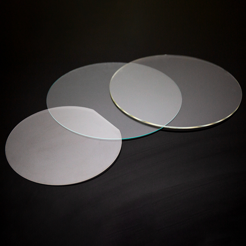 Quartz Wafers for Optical and Semiconductor ApplicationsCompare high-purity quartz wafers with low thermal expansion and UV-to-NIR transparency for waveguide, MEMS, semiconductor, and optical component uses.View Product →
Where Sapphire Wafers Earn Their Price
Sapphire substrates pay for themselves in four application families, each with a different dominant specification.
GaN LED and microLED epitaxy
Two to six inch c-plane wafers carry the light-emitting stack. Offcut control and front-side roughness influence crystal quality, and therefore external quantum efficiency, more than any other incoming parameter.
Radio frequency and silicon-on-sapphire
An insulating substrate cuts parasitic capacitance in switches and filters. Here the drawing is dominated by thickness uniformity and surface flatness rather than optical transmission.
Optical windows and sensor covers
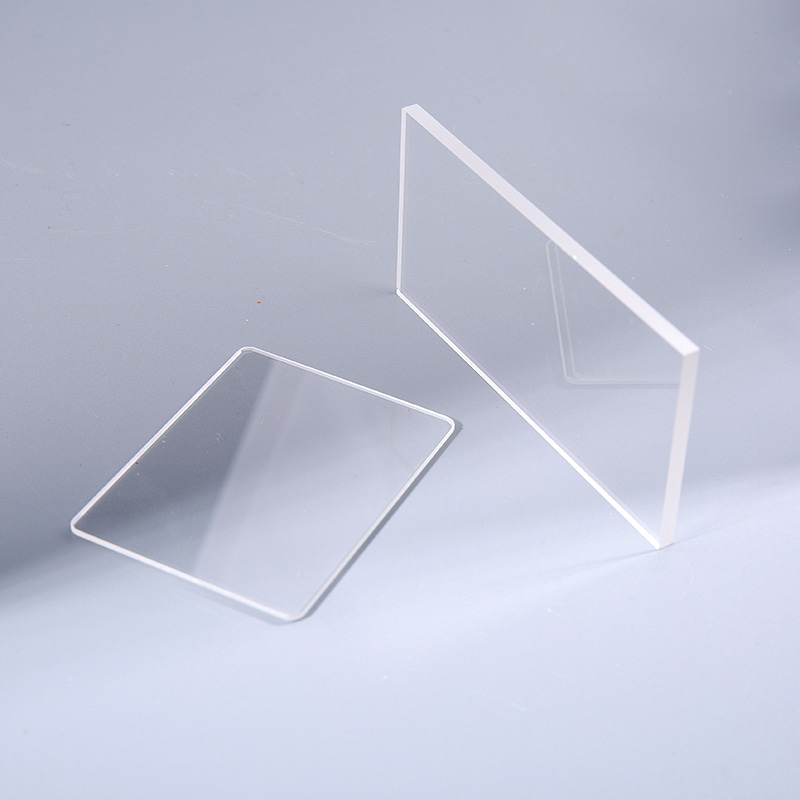
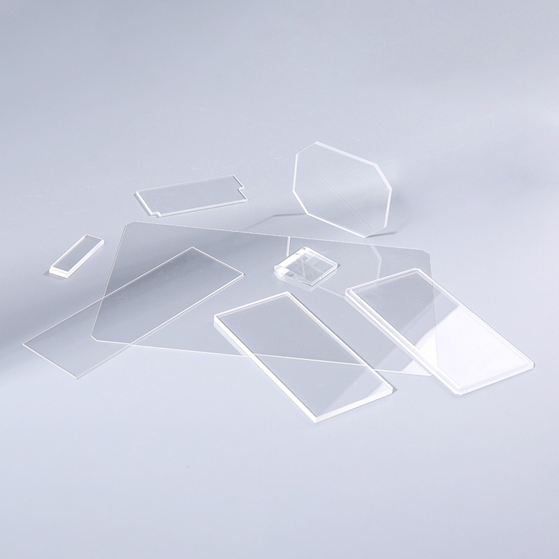
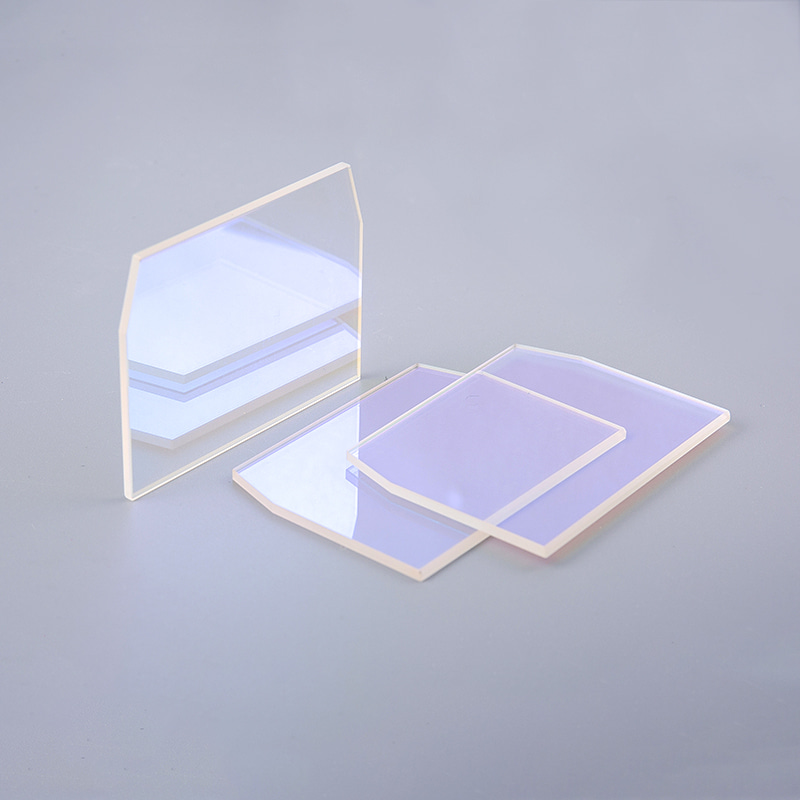
Sapphire transmits from the visible to about 5.5 micrometers and resists scratching in abrasive environments, so it appears in infrared windows, LiDAR covers, and hardened camera ports. The range of sapphire wafer applications across electronics and optics goes well beyond lighting.
Carrier and dummy wafers
High-temperature processes reuse sapphire carriers because the material does not soften or outgas. Repolishing extends service life where contamination rules allow it.
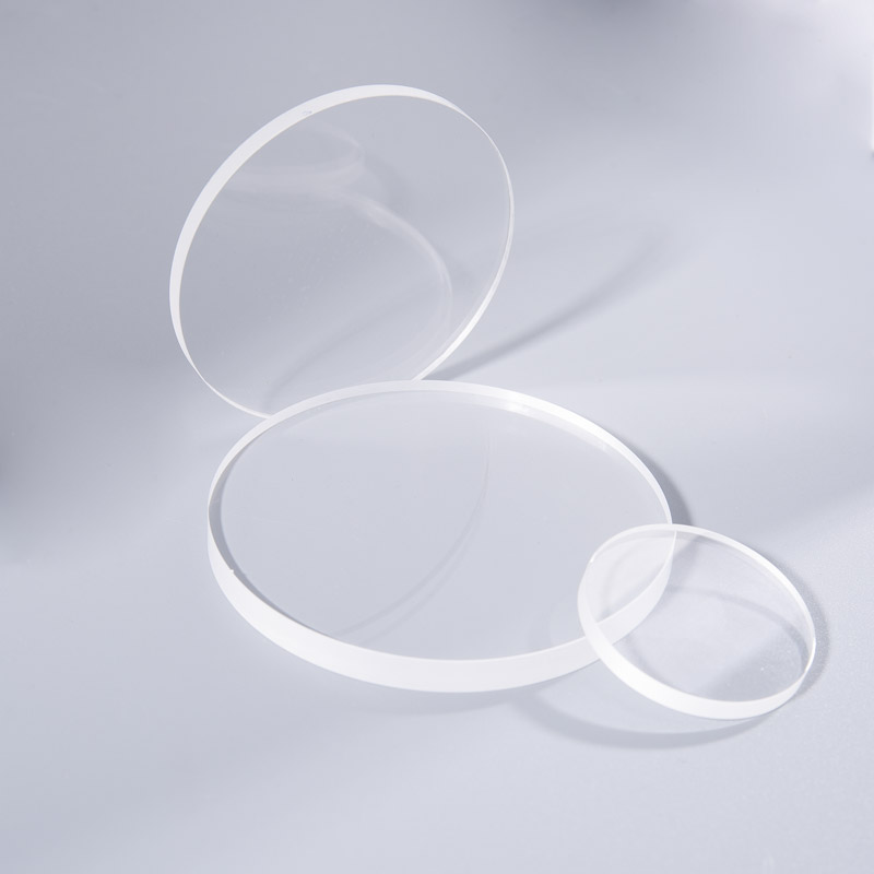
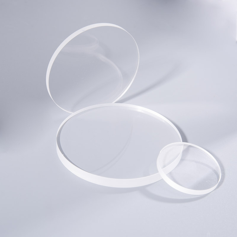 Sapphire Optical Windows for Protective and Filtering UsesView sapphire window substrates offering scratch resistance, high transparency, and wavelength filtering for lasers, photodiodes, and fiber-optic communication systems.View Product →
What to Verify Before You Order
Five checks catch most of the problems before a lot reaches your incoming inspection bench.
If a specification is ambiguous, resolve it at the drawing stage. Send your drawing and quantity to our engineering team and the orientation, finish, and inspection method can be fixed before quotation rather than after delivery.
Frequently Asked Questions
Is a sapphire wafer the same thing as a sapphire window?
No, the emphasis differs. A wafer is judged on total thickness variation, particle cleanliness, and an epitaxy-ready front surface, while a window is judged on transmission, surface quality over a defined aperture, and edge finish. Both can be cut from the same boule.
Can sapphire wafers be reused?
Carrier and dummy wafers can be repolished several times when contamination is controlled. Epi-ready wafers generally cannot, because the polished surface and the flatness budget are consumed by the first growth run.
Which thickness should I order?
Follow the diameter. Around 430 micrometers at 2 inch, 650 at 4 inch, and 1 mm or more at 6 inch are common starting points. Thinner wafers reduce thermal mass but raise breakage risk during handling and transport.
Do I need an offcut?
For GaN grown by MOCVD on c-plane, a small offcut near 0.2 degrees is typical. If your process is not sensitive to step structure, a nominal on-axis wafer is easier to source and usually less expensive.

 苏公网安备32041102000130号