
 Search
 en
en English
 日本語
日本語 русский
 Español
 Deutsch
 中文简体
中文简体Content
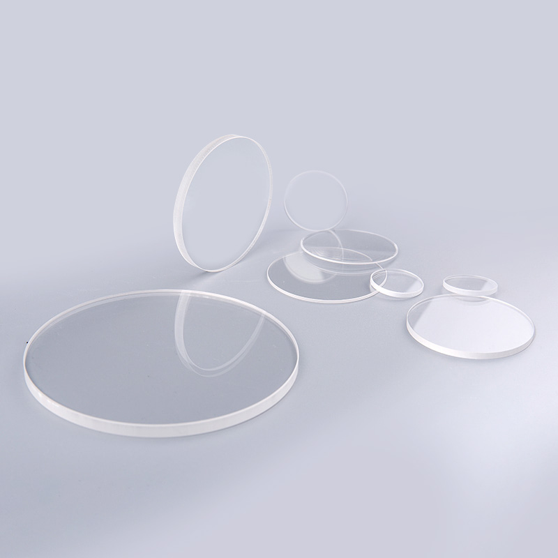
An optical wafer is a thin, parallel-sided plate of glass, fused quartz, or sapphire that has been lapped and polished until both faces meet micron-level thickness, flatness, and surface-quality tolerances. It sits at the front of the build for image sensors, filter stacks, waveguides, and wafer-level optic arrays, where a few microns of total thickness variation can shift focus, distort a wavefront, or push a coating run out of specification.
Most projects reach this category with three questions attached: which material, which tolerances, and which supplier can hold those tolerances across a production run instead of on one polished sample. The sections below follow that order.
What Exactly Counts as an Optical Wafer
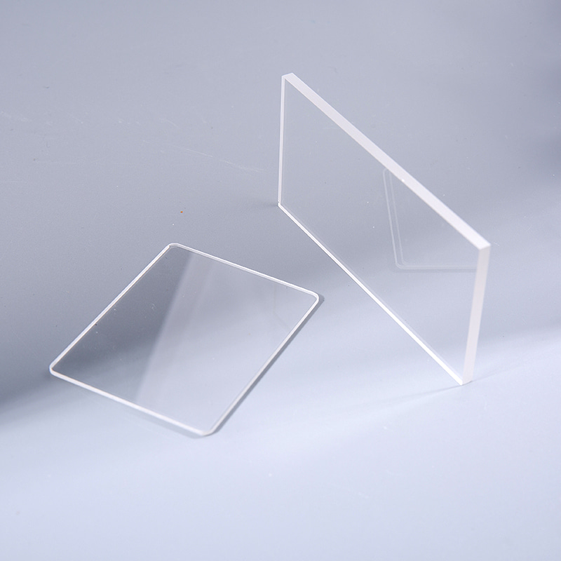
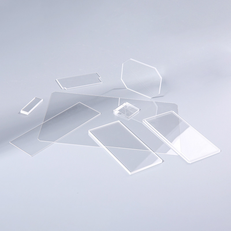
In purchasing terms, an optical wafer is a bare or coated optical substrate supplied in a round, square, or custom contour format, with dimensional and surface requirements written on the drawing rather than implied by a material name.
An optical wafer is a thin, flat substrate, usually 0.3 mm to 3 mm thick, made from glass, fused quartz, or sapphire and processed to a specified total thickness variation, flatness, and surface roughness. It works as the optical or structural base layer of a device, not as a finished mounted component.
That distinction changes quotations. An optical window is normally thicker, often mounted in a frame, and sold as a finished part. A wafer is thinner, handled in cassettes or gel packs, and frequently moves through downstream steps such as coating, bonding, dicing, or lithography. Suppliers who machine windows well do not automatically hold wafer tolerances, because thin parts deflect under polishing pressure and lose flatness quickly.
Glass, Quartz, and Sapphire Optical Wafers Compared
Choose the material by wavelength band first, then by the thermal and mechanical environment, then by cost.
| Property | Borosilicate glass | Fused quartz | Sapphire |
| Useful transmission | 350 - 2000 nm | 185 - 2500 nm | 150 - 4500 nm |
| Mohs hardness | 5.5 | 7 | 9 |
| CTE (ppm/K) | 3.3 | 0.5 | 5.3 - 8.7 |
| Refractive index at 589 nm | 1.47 | 1.46 | 1.77 |
| Thermal shock resistance | Moderate | High | Very high |
| Typical wafer thickness | 0.5 - 3.0 mm | 0.3 - 6.0 mm | 0.3 - 2.0 mm |
| Indicative relative cost | 1x | 3 - 5x | 8 - 15x |
| Common fit | Displays, sensors, general visible optics | UV optics, semiconductor process, high-temperature fixtures | IR windows, harsh-environment sensing, wear surfaces |
Sapphire earns its price in infrared and abrasive environments, not in the visible band. If a system works between 400 nm and 1000 nm, never sees a thermal cycle above 150 C, and is not exposed to aggressive cleanroom chemistry, glass or quartz usually does the same optical job for far less. Sapphire becomes the cheaper option the moment a scratched or etched window stops a production line.
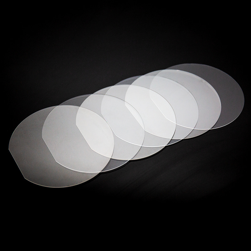 Custom Sapphire Wafers for Harsh Optical and Substrate UsesWhere infrared, abrasive, or high-temperature exposure makes glass or quartz insufficient, these custom sapphire wafers provide hardness, chemical resistance, and electrical isolation.View Product →
Fused quartz is not one material. Optical grades differ in OH content, bubble class, and index homogeneity, while semiconductor grades add tight limits on metallic impurities. Specifying quartz without a grade, a transmission curve, and an inclusion class is one of the most common reasons a first shipment fails incoming inspection.
Specifications to Lock Down Before Ordering
Five numbers decide whether a wafer will behave in your system: thickness, thickness tolerance, total thickness variation, flatness, and surface roughness, with scratch-dig close behind.
- Thickness and tolerance. Commercial work runs at +/- 0.05 mm, precision at +/- 0.025 mm, and small parts can be held to +/- 0.01 mm.
- Total thickness variation. The gap between the thickest and thinnest point. It drives wavefront error, coating uniformity, and focus shift across a wafer-level array.
- Flatness. Reported in waves at 633 nm, where a quarter wave equals roughly 158 nm of deviation. Always state the measurement aperture, because a value taken over 80 percent of the diameter is a weaker claim than a full-aperture number.
- Surface roughness. Ra sets scatter and laser damage threshold. Standard polishing lands near 0.5 nm; superpolished surfaces reach 0.2 nm and below with longer cycles.
- Scratch-dig. Callouts such as 60/40, 40/20, or 10/5 define allowed scratches and pits. Tightening from 40/20 to 10/5 often costs more than tightening thickness tolerance.
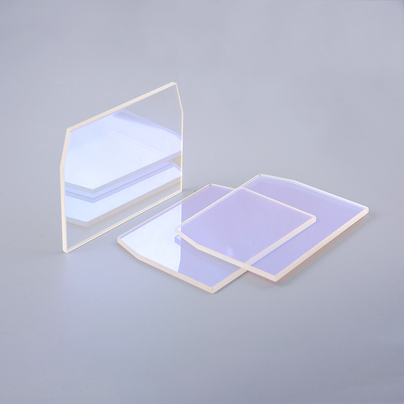
- Parallelism, edge, and coating. Wedge matters for etalons and beam splitters, edge chips matter for cassette handling, and coating adhesion matters for anything cleaned repeatedly.
Write down how each number will be measured. A drawing that says high quality polish leaves the supplier to deliver their own standard, and the argument then happens at incoming inspection instead of at quotation.
How Optical Wafers Are Manufactured
Every wafer moves through material preparation, shaping, lapping, polishing, cleaning, and metrology, and each step can only remove what the previous step left behind at a predictable rate.
- Material preparation. Glass sheets, quartz ingots, or sapphire crystals are cut or cored into rough blanks. Annealing state and internal stress are confirmed before machining, because stress released later shows up as bow.
- Shaping. Core drilling, CNC contouring, or laser cutting produces the outline and leaves stock for lapping. Holes and slots are cut at this stage.
- Lapping and fine grinding. Removes saw damage and establishes parallelism. Stock removal per side depends on part size and can exceed 100 microns.
- Polishing. Pitch or pad polishing, single or double sided, sets flatness and roughness. A batch can run for hours, and fixture design often matters more than the slurry.
- Cleaning. Ultrasonic and detergent stages, deionized rinsing, and controlled drying prevent watermarking and residue that later becomes a coating defect.
- Metrology. Interferometry for flatness, white-light or stylus instruments for roughness, spectrophotometry for transmission, and microscopy for scratch-dig and edge chips.
- Packaging. Cleanroom bagging, wafer carriers, and edge protection decide whether a good wafer arrives in usable condition.
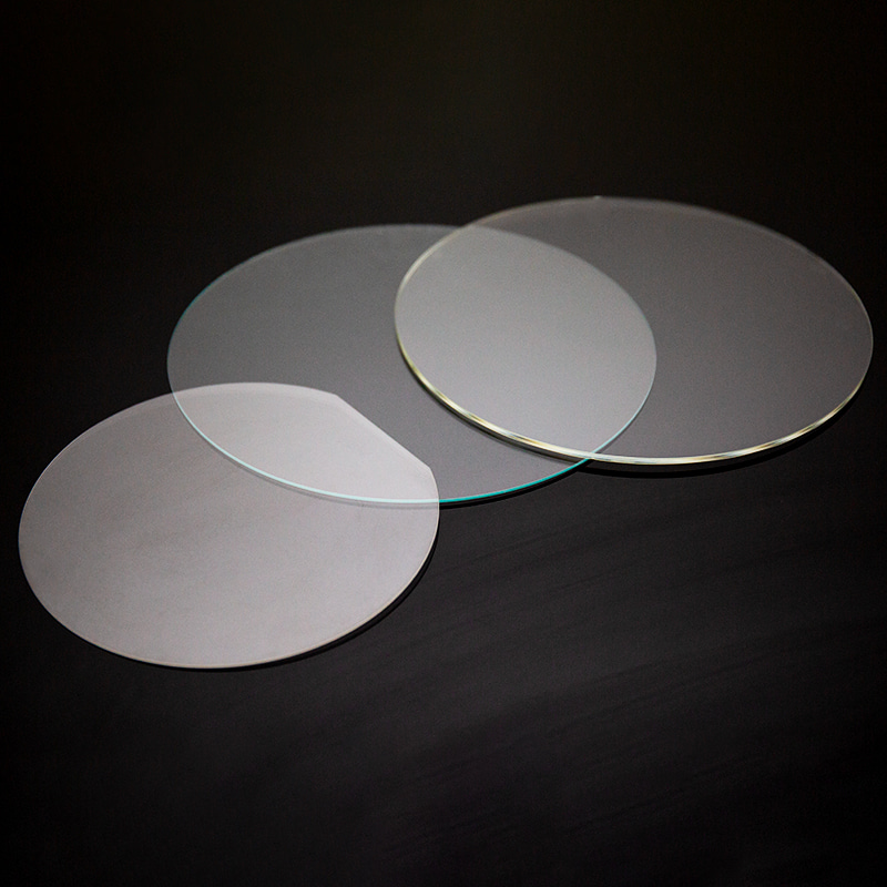 Custom High-Precision Quartz Wafers for Optical and Semiconductor ApplicationsThese quartz wafers combine low thermal expansion and high transmission for PLC, MEMS, photonics, and semiconductor work where lapping, polishing, and flatness control matter.View Product →
Flatness is a process capability, not a sorting step. Moving a 100 mm part from half-wave to quarter-wave can double polishing time and require new fixturing, which is why price does not scale linearly with tolerance. HLL's notes on how flatness is controlled during optical wafer fabrication cover the measurement side in more detail.
Where Optical Wafers Are Used
Optical wafers appear wherever a device needs a flat, stable, transparent base layer: image sensors, LiDAR paths, semiconductor process tools, infrared windows, and display or lighting systems.
Semiconductor and photonics
Quartz wafers act as carriers, substrates, and optical elements in lithography and inspection equipment, where purity and low metallic contamination matter as much as flatness.
Sensing and imaging
Cover wafers for CMOS sensors, filter stacks, and wafer-level optic arrays depend on uniform thickness, because variation across the wafer becomes focal shift from die to die.
Infrared and harsh environments
Sapphire serves infrared laser windows, thermal imaging, and industrial sensing where abrasion, chemical exposure, and thermal cycling would damage glass.
Glass wafers carry the widest range of volume applications, from camera modules and touch sensing to lighting diffusers and microfluidic carriers, because the material is inexpensive and the polishing process is well established.
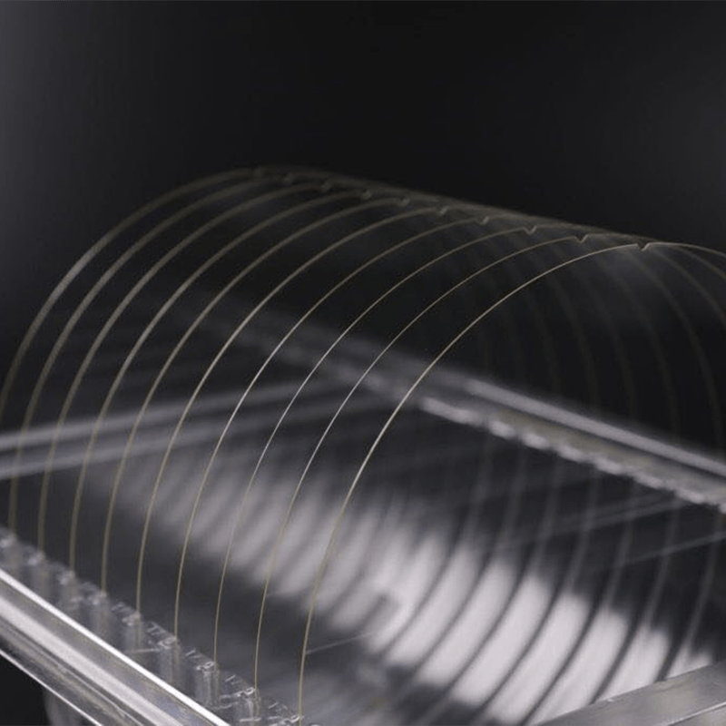 Custom Glass Wafers for Optics, MEMS, and Semiconductor PackagingFor camera modules, sensors, and patterned optical arrays, these custom glass wafers offer transparency, low fluorescence, and stable substrates in 4- to 12-inch sizes.View Product →
Array uniformity is the hidden requirement. When one wafer carries hundreds of lenses or filters, consistency across the whole part matters more than the best value measured at the center, and the yield loss usually shows up at assembly rather than at incoming inspection.
Sourcing, Quality, and Delivery Considerations
Qualify the process rather than the brochure: ask for capability data on the exact material, format, and tolerance combination you are buying, and treat certificates as a baseline rather than as proof.
Signals of a capable supplier
- Capability studies on comparable parts, not a single best sample
- In-house lapping, polishing, and metrology rather than assembly only
- Named raw material grade with lot traceability
- Inspection data shipped with the parts
- A written change-notification process
Warning signs
- Any tolerance accepted without a discussion of polishing limits
- Flatness quoted without an aperture or wavelength
- No interferometer or roughness measurement on site
- Samples polished by hand while production is outsourced
- No answer on packaging, edge protection, or cleanliness class
On documentation, ISO 9001 and ISO 14001 are the usual baseline, and IATF 16949 becomes relevant when the wafer feeds an automotive program. Medical and semiconductor buyers normally add RoHS and REACH declarations plus a cleanliness statement. Lead time follows tolerance as well: standard round wafers in glass and quartz commonly ship in two to three weeks, while custom contours with slots or holes and first-article approval usually run five to eight weeks.
The least expensive wafer is the one that passes incoming inspection on the first shipment and on the tenth, with the same inspection data attached each time.
If the drawing is still open, send the material, format, and target tolerances to the engineering team and ask for a capability statement against each line before the order is placed.
Frequently Asked Questions
What is the difference between an optical wafer and an optical window?
A wafer is thin, usually under 3 mm, handled in cassettes, and used as the base layer for further device processing. A window is thicker, normally mounted in a frame or housing, and sold as a finished transmissive or protective part. Both can use the same materials and similar surface finishes.
What sizes and thicknesses are realistic?
Round wafers run from 25 mm to 200 mm in diameter, and square panels reach roughly 300 mm on a side. Thickness depends on material: glass and sapphire typically sit between 0.3 mm and 3 mm, while quartz can go thicker for structural use. Below 0.3 mm, bow, edge chipping, and handling become the limiting factors rather than polishing.
How do I choose between glass, quartz, and sapphire?
Start with the wavelength band, then add the thermal and mechanical environment, then apply cost. Glass covers the visible range economically, fused quartz extends into the ultraviolet and holds shape through thermal cycling, and sapphire covers the infrared plus abrasive or chemically aggressive settings.
What flatness can a supplier hold in volume production?
On 50 mm to 100 mm parts in glass or quartz, a quarter wave at 633 nm is a routine target for an experienced polisher, and one-tenth wave is achievable on selected parts at the cost of longer cycles and lower yield. Ask for the distribution across a batch instead of the best single result.
Match the material to the wavelength band, fix the five key numbers on the drawing, and qualify the polishing process before you negotiate the price.

 苏公网安备32041102000130号