
 Search
 en
en English
 日本語
日本語 русский
 Español
 Deutsch
 中文简体
中文简体Content
- 1 What Is an Optical Wafer?
- 2 Glass, Quartz, or Sapphire: Choosing the Wafer Material
- 3 Specifications to Lock Down Before Requesting a Quote
- 4 How Flatness Is Achieved and Verified in Production
- 5 Where Optical Wafers Are Used
- 6 Common Procurement Risks and How to Avoid Them
- 7 Working With an Optical Wafer Manufacturer
A borosilicate wafer and a sapphire wafer can share the same 100 mm diameter and 1.0 mm thickness, yet one costs a fraction of the other and survives a very different set of working conditions. That gap is where most wafer purchasing mistakes are made. In practice, the right optical wafer comes down to three decisions made in this order: choose the material for its transmission, hardness, and thermal behavior; define flatness and surface-quality figures the downstream process can actually tolerate; and require inspection data that proves both before shipment. The sections below work through each decision in turn.
What Is an Optical Wafer?
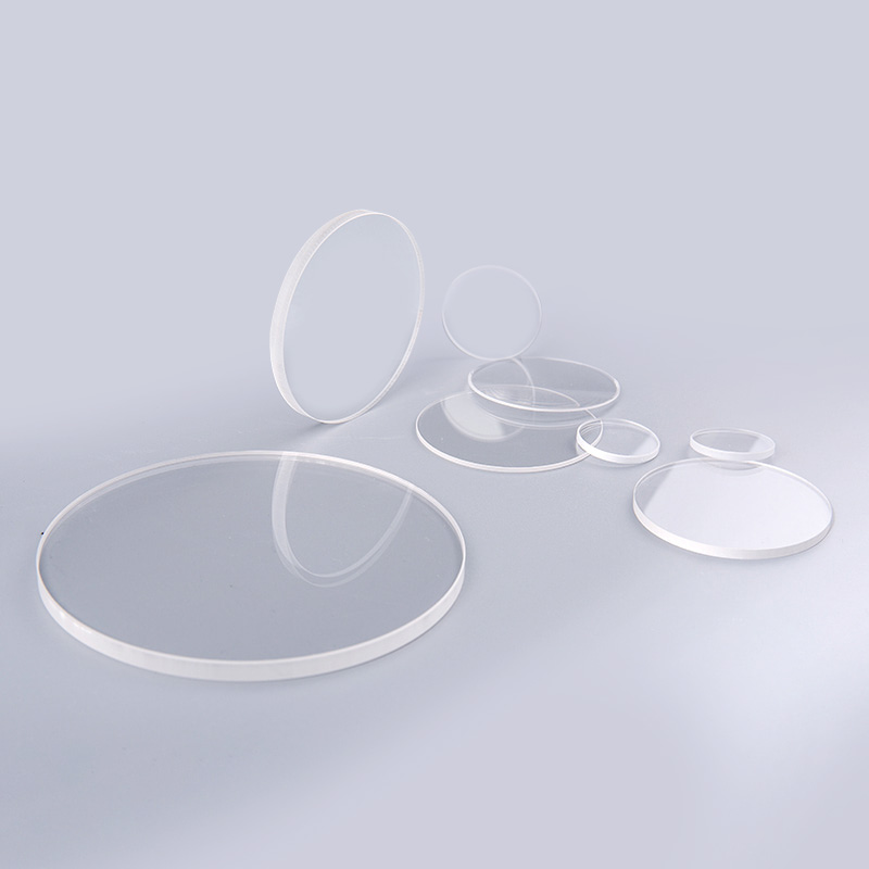
An optical wafer is a thin disc of optical-grade material, typically glass, fused quartz, or single-crystal sapphire, produced to tight tolerances on thickness, flatness, and surface quality. Unlike a finished optical window, which is installed directly into a beam path, a wafer is usually a substrate: a starting surface that will be coated, patterned, bonded, or diced during downstream processing.
Standard diameters run from 25.4 mm (1 inch) to 300 mm, with thicknesses commonly between 0.5 and 1.1 mm, though custom sizes are routine in industrial optics. Five parameters separate a usable wafer from a rejected one:
- Total thickness variation (TTV): the difference between the thickest and thinnest points across the polished surface.
- Bow and warp: deviations of the wafer mid-plane from flat, usually caused by residual stress left by grinding or lapping.
- Surface quality: scratch-dig grades such as 40-20 or 20-10 per MIL-PRF-13830, which limit allowable scratches and digs.
- Surface roughness: polished wafers typically reach Ra below 1 nm, and double-side polished stock below 0.5 nm.
- Edge condition: chamfer geometry and chip limits, which drive breakage rates during handling and dicing.
Glass, Quartz, or Sapphire: Choosing the Wafer Material
Material choice dominates cost and performance more than any other wafer decision. The table below compares the property ranges that drive selection, and the notes after it explain where each material earns its place.
| Property | Borosilicate Glass | Fused Quartz | Sapphire (Single Crystal) |
|---|---|---|---|
| Usable transmission range | ~350 nm to 2.5 μm | ~180 nm to 3.5 μm, with strong UV transmission | ~150 nm to 5.5 μm, covering UV through mid-infrared |
| Hardness (Mohs) | ~5.5 | ~5.5 to 6.5 | 9, harder than any common optical material except diamond |
| Thermal expansion | ~3.3 ppm/K | ~0.5 ppm/K, very low | ~5.3 to 8 ppm/K, direction-dependent |
| Thermal conductivity | ~1 W/m·K | ~1.4 W/m·K | ~25 to 40 W/m·K, excellent heat spreading |
| Relative cost | Low | Moderate | High |
| Typical wafer applications | MEMS bonding substrates, carriers, display optics | Photomask blanks, UV optics, semiconductor process plates | GaN LED epitaxy, IR windows, harsh-environment sensors |
When the choice narrows to the two most frequently compared options, the decision usually turns on UV transmission and thermal stability rather than price alone. We cover that pairing in detail in our comparison of quartz vs. glass optical wafers.
Glass Wafers: The Workhorse for Bonding and Carriers
Glass wafers, usually borosilicate or similar optical glasses, are the most cost-effective option where extreme transmission or hardness is not required. Their thermal expansion sits close enough to silicon for anodic bonding, which makes them standard substrates for MEMS pressure sensors and encapsulated devices. They also serve as carrier wafers during thin-device handling and as base substrates for patterned optics. The limits are real: weaker ultraviolet transmission than fused quartz, lower thermal shock resistance, and a surface that scratches more easily through repeated handling cycles.
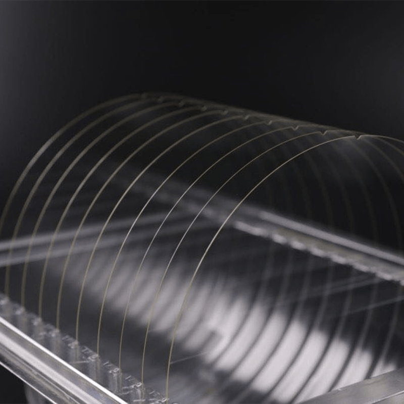 Glass Wafers for MEMS, Sensor and Optical SubstratesBorosilicate and similar glass wafers offer low cost, transparency, and thermal expansion close to silicon for anodic bonding. This makes them worth reviewing for MEMS sensor substrates, carrier wafers, and patterned optics where extreme UV transmission or hardness is not required.View Product →
Quartz Wafers: Low Expansion and Deep-UV Performance
Fused quartz wafers pair very low thermal expansion, roughly 0.5 ppm/K, which is an order of magnitude below most glasses, with strong transmission deep into the ultraviolet. That combination explains their role as photomask blanks, UV optical substrates, and process plates inside semiconductor equipment. One purchasing trap deserves attention: "quartz" can mean amorphous fused quartz or piezoelectric crystalline quartz, and the two differ substantially in price, machinability, and application. Confirm which one the process actually needs before requesting quotes.
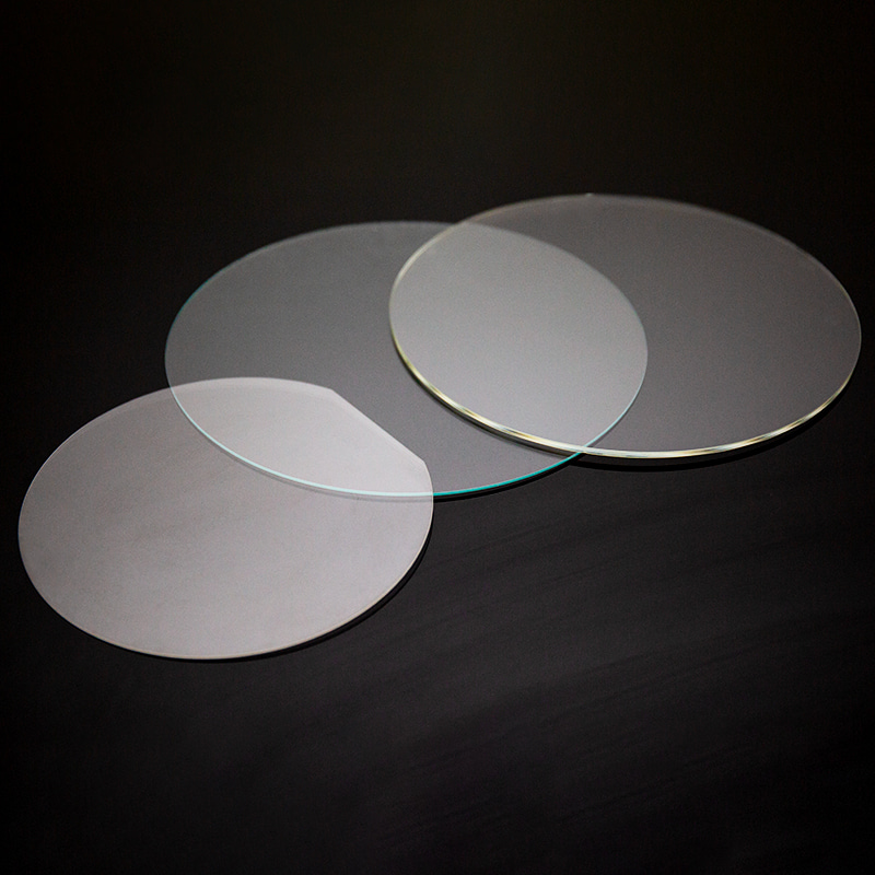 Fused Quartz Wafers with Low Expansion and UV TransmissionFused quartz wafers combine thermal expansion around 0.5 ppm/K with strong transmission deep into the ultraviolet. They are worth viewing for photomask blanks, UV optics, and semiconductor equipment process plates, provided the process needs amorphous rather than crystalline quartz.View Product →
Sapphire Wafers: Hardness and Harsh Environments
Single-crystal sapphire costs more per wafer and machines far more slowly than glass or quartz, but nothing else in common optical use combines 9-Mohs hardness, spectral coverage from roughly 150 nm to 5.5 μm, and high thermal conductivity. It is the default substrate for gallium nitride LED epitaxy, a standard choice for mid-infrared windows and sensors exposed to abrasion or high temperature, and increasingly common in automotive optics. Because sapphire properties depend on crystallographic orientation, the cut, whether C-plane, R-plane, or another plane, must be stated explicitly on the drawing.
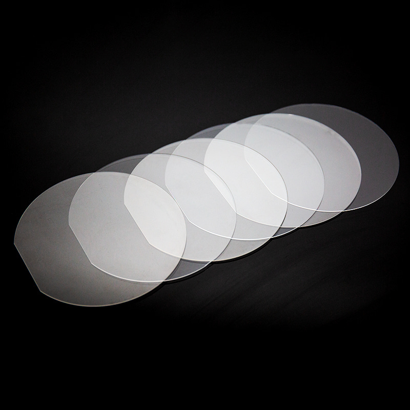 Sapphire Wafers for LED Epitaxy and Harsh Optical UsesSingle-crystal sapphire offers 9-Mohs hardness, transmission from roughly 150 nm to 5.5 μm, and high thermal conductivity. This product is worth considering for GaN LED epitaxy, mid-infrared windows, and sensors facing abrasion or high temperatures, with the crystal plane specified.View Product →
Specifications to Lock Down Before Requesting a Quote
Most wafer rejections trace back to specifications that were never stated, not to manufacturing failures. Put a number on each item below before sending a request for quote:
- Diameter and thickness with tolerances, for example 100 mm ±0.1 mm diameter and 1.0 mm ±0.05 mm thickness, rather than "nominal 100 mm".
- Flatness limits matched to the application: lithography substrates may need total thickness variation under a few microns across the clear aperture, while general optical use tolerates looser values.
- Surface quality expressed as scratch-dig, typically 40-20 for general use and 20-10 where scattered light matters.
- Polishing format, single-side or double-side, since both surfaces matter when the wafer feeds an optical path or a precision chucking operation.
- Crystal orientation for sapphire or cut type for crystalline quartz, shown on the drawing rather than assumed.
- Cleaning, packaging, and documentation requirements, including whether each lot needs interferometer flatness maps and a certificate of conformance.
How Flatness Is Achieved and Verified in Production
A wafer's flatness is built through a fixed sequence: sawing the blank, grinding to near-final thickness, lapping to remove subsurface damage, then polishing, single-side or double-side, to bring the surface into specification. Each stage must remove the damage left by the one before it, and rushing a step shows up as scratches or residual stress at final inspection.
Verification matters as much as processing. TTV, bow, and warp are commonly measured with non-contact optical scanning, while surface figure is confirmed by interferometry at a stated wavelength. A flatness figure quoted without an aperture and a wavelength, such as "λ/10 flat" with no conditions attached, cannot be compared against another supplier's number, so put both on the drawing.
Where Optical Wafers Are Used
Wafer-based optics appear in far more industries than semiconductor manufacturing alone:
- Semiconductor production: photomask substrates, inspection optics, and carrier wafers for handling thin devices.
- Optical sensors in imaging systems: wafer-level processing produces sensor windows, filters, and microlens substrates in batches with consistent surface quality.
- MEMS devices: glass wafers anodically bonded to silicon form pressure sensors, microphones, and resonators.
- Ultraviolet and infrared systems: fused quartz serves deep-UV lithography and spectroscopy, while sapphire covers mid-IR windows and high-temperature sensing.
- Automotive and LiDAR: dimensionally stable, hard substrates for emitter and receiver optics that must survive vibration and temperature swings.
Common Procurement Risks and How to Avoid Them
Four issues account for most of the trouble in wafer sourcing:
- Ambiguous flatness callouts. Every flatness figure needs an aperture, a wavelength, and a measurement method written on the drawing.
- Material mislabeling. Confirm whether "quartz" means fused amorphous material or crystalline stock, and whether a "glass" wafer is borosilicate, aluminosilicate, or another composition, because each differs in expansion and transmission.
- Thermal expansion mismatch in bonded assemblies. A glass wafer bonded to silicon must be chosen for expansion compatibility, or the bond cracks during thermal cycling.
- Missing inspection data. Without interferometer maps or a certificate of conformance, surface problems only appear after downstream processing, when a rejected wafer costs the most.
Working With an Optical Wafer Manufacturer
Buyers evaluating suppliers need a short checklist: proven processing of all three wafer materials, demonstrated flatness-control capability, and a quality system audited to recognized standards. Changzhou Haolilai Photo-Electricity Scientific and Technical Co., Ltd. (HLL) has manufactured precision optical components since 1998 from a 35,000-square-meter facility in Changzhou's national high-tech zone, employing more than 300 people and exporting to over 20 countries. The company holds ISO 9001:2015, ISO 14001:2015, and IATF 16949 certifications, the last of which supports automotive supply chain work, and operates a provincial precision optical engineering center that backs custom wafer and substrate projects.
Wafer requirements vary widely between semiconductor, automotive, and laser applications, so the fastest route to accurate pricing is a drawing that carries the specifications listed above. HLL's engineering team reviews custom requirements and provides tailored optical solutions, and requests for quote or technical questions can be sent through the contact page.
The short version: pick the material for its optical and thermal properties, specify flatness and surface quality with numbers and measurement conditions, and demand inspection data with delivery. Buyers who follow that sequence avoid the most expensive failure modes in wafer sourcing and move from quote to qualified parts in fewer iteration cycles.

 苏公网安备32041102000130号